Research highlights
TEM is a versatile tool to study materials and devices down to the atomic scale. Far from simply being a very good microscope, the TEM can be considered as an in-house beam line, where imaging, diffraction, spectroscopy, and many other techniques can be combined to provide a comprehensive view of the sample unrivaled by any other facilities. The goal of the NORTEM infrastructure is to make these techniques available to the Norwegian research community. Below are some highlights from recent years.
Unraveling many-body effects in ZnO by Momentum-Resolved Electron Energy-Loss Spectroscopy (ω-q EELS)
Zinc oxide (ZnO) is a widely studied semiconductor due to its versatile application in electronics, optoelectronics, and nanotechnology. Understanding ZnO electronic and optical properties requires detailed insight into many-body interactions like excitons and plasmons. Momentum-resolved (ω-q) EELS allows for precise mapping and interpretation of excitonic and plasmonic behaviors, as well as interband transitions, as a function of energy loss and momentum transfer (i.e., their dispersion) in ZnO. This offers deep insights into its many-body interactions as well as anisotropic electronic properties.

Energy- and momentum-resolved ω-q EELS maps of ZnO are shown along the ΓA (∥c), ΓM (⊥c), ΓK, and KMK directions. This reveals the momentum-dependent dielectric response of ZnO, demonstrating its complex response. The dispersion associated with the band gap onset is indicated by the yellow arrows.
Credit: Cana Elgvin
For more details, refer to this article: https://doi.org/10.1103/PhysRevB.109.115153
Plasmon mapping of gold nanoparticles by Monochromated Electron Energy-Loss Spectroscopy (EELS)
Gold nanoparticles are widely used in applications such as biomedicine and sensing due to their unique optical and electronic properties. They are also of interest in photovoltaics and photocatalysis. Their ability to create localized plasmon resonances makes them valuable for enhancing light interactions at the nanoscale. STEM-EELS is particularly useful for mapping plasmon modes in these systems as it provides high spatial and energy resolution, enabling detailed analysis of the local electromagnetic field distribution, offering insights that are not easily obtained through traditional optical techniques.

Annular dark field (ADF) STEM images and EELS spectrum imaging maps of gold nanoparticle clusters. The ADF images mark different regions of interest (blue and red squares), corresponding to distinct plasmonic modes detected through EELS. The energy loss spectra indicate resonance peaks at specific energies: 1.4 eV and 2.2 eV for the left cluster, and 1.7 eV and 2.5 eV for the right cluster. The corresponding SI maps illustrate the spatial distribution of these modes, revealing localized plasmonic modes with specific energies. These results highlight how plasmonic resonances can be investigated at the nanoscale for single and clusters of nanoparticles using STEM-EELS.
Credit: Fredrik S. Hage
Atomic-scale chemical analysis of perovskite-based structures using Electron Energy Loss Spectroscopy (EELS)
Exsolution is a phase transition that enables controlled growth of anchored nanoparticles on metal oxide support. Such exsolved nanoparticles with transition metals are observed to enhance the catalytic properties and counteract agglomeration, which both enhance their performance in novel energy storage and conversion technologies. A-site deficient SrTiO3 with the inclusion of the exsolving transition metal, e.g., La₀.₂Sr₀.₇Ti₀.₉Ni₀.₁O₃ (LSTN), is the most common material system. LSTN holds many point defect that are important to identify to understand the phase transition to enable better control of the growth.

Using STEM-EELS, the composition of a LSTN perovskite structure is examined at the atomic level. Core-loss EELS maps and their ratio helps visualize defects associated with specific substituents. A-site vacancies, oxygen octahedra, and Ni defect type are key to understand the exsolution process.
Credit: Andreas Rosnes
In-situ annealing studies of double γ/β-Ga2O3 polymorph structure by electron diffraction and high-resolution STEM imaging
Polymorph transitions in Ga₂O₃ are being intensively studied due to its growing importance in power electronics and UV photonics. Double polymorph γ/β-Ga₂O₃ structures were created by implanting (010)-oriented β-Ga₂O₃ single crystal wafers with either ²⁸Si⁺ or ¹⁹⁷Au⁺, followed by in situ annealing electron microscopy, which provided unprecedented accuracy in assessing the γ-to-β polymorph transition.

Credit: Javier G. Fernandez
For more details, refer to this article: http://dx.doi.org/10.1039/D3MA01011B
Analysis of disordered structure of silicon-based anode materials using Electron Pair Distribution Function
Silicon (Si) and SiC-based anodes in lithium-ion batteries offer high capacity but experience volume expansion during lithiation, impacting their performance. Electron Pair Distribution Function (ePDF) is a powerful technique for investigating the local atomic structure of Si and SiC-based anodes during this process, providing insights into structural changes and volume expansion. ePDF is especially effective for studying materials that lack long-range order, such as nanomaterials, glasses, and disordered crystalline structures. By analyzing atomic pair distributions, ePDF reveals detailed information about atomic arrangement and bonding, making it invaluable for understanding complex materials where traditional crystallographic methods fall short.

The plots show the reduced Pair Distribution Function G(r) from pure Si (purple) and SiCx (grey) sample, which represents the degree of correlation between atom pairs as a function of interatomic distance (r). Peaks in the G(r) plot correspond to preferred atomic separations, indicating structural features or bond lengths within the material.
Credit: Anuj Pokle
Probing defects in Iron-doped ZnO using contrast-enhanced TEM imaging techniques
Iron doping in ZnO can induce the formation of inversion domain boundaries (IDBs) - structural defects that influence the material’s functional properties. Engineering these defects is crucial for optimizing the functional properties of oxide semiconductors. By using complementary electron microscopy techniques, we visualize and analyze these complex defect networks, guiding rational design and optimization of doped ZnO and related materials.

Credit: Phuong Dan Nguyen
For more details, refer to this article: http://dx.doi.org/10.1039/d2na00849a
Studies of crystal structure

Using the high resolution capabilities of the FEI Titan, atomic scale details of the crystal structure of materials can be studied. Here, the interface between a Zn2GeO4 nanocrystal and the surrounding ZnO is studied, to further understand the how embedded nanostructures can enhance the light harvesting properties of photovoltaic devices.
Granerød et al Nanotechnology 30 225702 (2019).
Image licensed under CC-BY 3.0.
Imaging of defects

The properties of materials can be significantly altered by defects in the perfect crystal lattice. Identifying these and understanding their formation and evolution is of central importance when tailoring materials' properties to the desired performance. In this example, the formation of stacking faults and their interaction with implanted nitrogen in ZnO was studied.
Bazioti et al. J. Phys. Chem. Lett. 10 4725 (2019).
Image ©2019 American Chemical Society. Reproduced with permission.
Optical properties
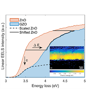
Monochromated Electron Energy Loss Spectroscopy (EELS) gives us access to 'a synchrotron in the TEM', allowing the unique combination of both high spatial resolution and spectroscopy in the IR to X-ray range. In this example, the Burstein-Moss shift and conduction band plasmons in Ga-doped ZnO were investigated, demonstrating that the charge carrier density in semiconductors can be measured with nanometer resolution.
Granerød et al. Phys. Rev. B 98 115301 (2018).
Image ©2018 American Physical Society. Reproduced with permission.
Composition analysis
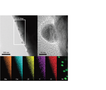
In catalytic and electrochemical applications, control of the composition and microstructure of the catalysts and electrodes is crucial. Here STEM imaging and chemical analysis by EDS were used to verify the structure and composition of ~20 nm active Ni particles in a protonic membrane reformer for production of high purity hydrogen.
Malerød-Fjeld et al. Nat. Energy 2 923 (2017).
Image ©2017 Springer Nature. Reproduced with permission.
Mapping of fields
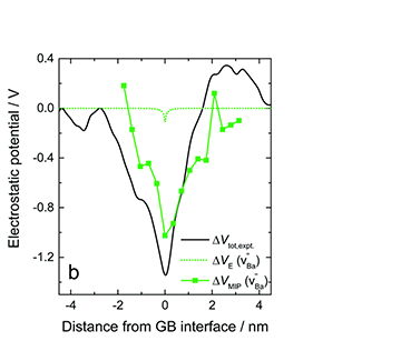
In addition to spectroscopy, imaging, and diffraction, several techniques can be used to measure and image intrinsic electric and magnetic fields in the sample. In this work in-line electron holography was performed using the JEOL 2100F to investigate the electrostatic potential across BaZrO3 grain boundaries. These measurements were successfully compared with models taking detailed compositional and structural information as input.
Bondevik et al. Phys. Chem. Chem. Phys. 21 17662 (2019).
Image ©2019 the PCCP Owner Societies. Reproduced with permission.
Nanoscale chemical states

Using core loss EELS, chemical binding information can be obtained down to the atomic scale. In this example, EELS was used to uncover clustering of nitrogen in a ZnO-GaN alloy, and to identify the covalent N-N bonding characteristic of molecular nitrogen, thereby demonstrating the formation of bubbles of nitrogen gas in the sample.
Bazioti et al. Phys. Chem. Chem. Phys. 22 3779 (2020).
Image licensed under CC-BY 3.0.