UiO MiNaLab is one of four cleanroom facilities within the national infrastructure, "The Norwegian Micro- and Nanofabrication Facility", NorFab, together with NTNU NanoLab, USN MST Lab and SINTEF MiNaLab. The UiO MiNaLab facility is open to all students and scientists at UiO, as well as external researchers and start-up companies.
Please visit our new UiO MiNaLab website for detailed information on access, available equipment/processes, and our services.
Contact
Lab Manager: Vegard Skiftestad Olsen
Research Infrastructure Coordinator: Eirini Zacharaki
Inquiries: norfab-minalab@smn.uio.no
Location: Gaustadalléen 23 C, 0373 Oslo, Norway
Technologies at UiO MiNaLab
Please visit our new UiO MiNaLab website for detailed information on technologies and equipment (including instrument specifications) available at UiO MiNaLab.
Synthesis and fabrication
- Physical vapor deposition (PVD):
- Magnetron sputtering (DC, RF, HiPIMS, Remote plasma)
- E-beam evaporation
- Thermal evaporation
- Chemical vapor deposition (CVD):
- Atomic layer deposition (ALD)
- Plasma-enhanced chemical vapor deposition (PECVD)
- Metal-organic chemical vapor deposition (MOCVD)
Material modification/processing
- Modification techniques:
- Ion implantation
- Processing:
- Laser cutter
- Cross-section polishing
- Maskless photolithography
- Tube furnace
- Rapid thermal annealing (RTA)
Material characterization
- Electrical and electrochemical
- Hall measurements (room-temperature, high-temperature and low temperature)
- 4-point probe
- Solar simulator
- Quasi-steady state photoconductance (QSSPC)
- Probe station (IV, CV)
- Scanning spreading resistance microscopy (SSRM)
- Optical and imaging
- Cathodoluminescence (CL)
- Spectrophotometer (UV-VIS)
- Fourier-transform infrared spectroscopy (FTIR)
- Ellipsometry
- Scanning electron microscopy (SEM)
- Optical microscope
- Structure, composition and topography
- X-ray diffraction (XRD)
- Scanning probe microscopy (SPM)
- Stylus profiler
- SEM-based energy dispersive spectroscopy (EDS)
- Rutherford backscattering spectrometry (RBS)
- Ultraviolet photoelectron spectroscopy (UPS)
- X-ray photoelectron spectroscopy (XPS)
- Angular-resolved photoemission spectroscopy (ARPES)
- Low-energy electron diffraction (LEED)
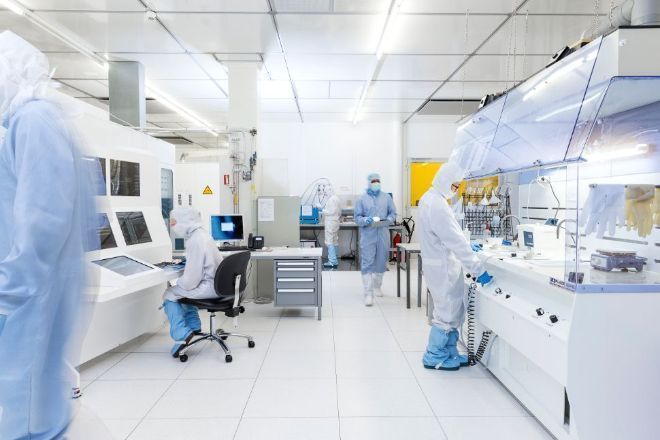
Photo gallery