About the Project
Two-dimensional (2D) materials are emerging as a novel class of functional materials for the miniaturization of electronic and electrochemical devices. They pave the way for electrochemical capacitors with energy densities approaching that of Li-ion batteries due to stacking efficiency, photovoltaic devices with strong light matter interactions and novel transistor architectures - technology that would represent a significant breakthrough for renewable energy storage and conversion. The project seeks fundamental understanding of the defect chemistry and functional properties of 2D materials, encompassing charged point defects as well as clusters in the material and at its highly influential interfaces (surface, edge, inter-layer and substrate).
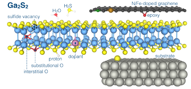
The project builds upon a fabrication procedure recently demonstrated by the applicants for 2D MoS2, involving PVD techniques and post treatment in H2S at elevated temperature. MoS2 and Ga2S2 will serve as model systems, and other 2D materials and ultra thin films will be pursued, e.g., WSe2, MnO2, TiOxNy. First-principles calculations will be combined with Advanced characterization of the prepared 2D films to elucidate the defect chemistry of the materials, including charge compensation mechanisms for intrinsic and extrinsic defects in the material and interfaces. An electrical characterization setup for 2D films under controlled temperature and atmosphere will be developed. 2D heterostucture devices will be constructed to demonstrate application Properties.
The project will be managed by SINTEF with partners at University of Oslo and University of Luxembourg
Financing
The project is funded by Research Council of Norway, Young Research talent under FRINATEK program, project number 262274