About the project
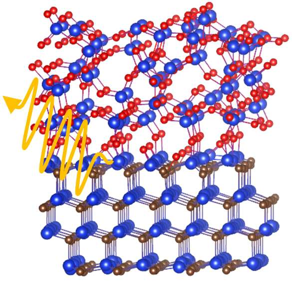
The field of quantum technology (QT) aims to exploit the most exotic consequences of quantum mechanics for real-world applications. However, it has proven challenging to strike the balance between control of the quantum state, robustness to noise, and, importantly, scalable material and processing. Thus, there is an ongoing race to discover and characterize new quantum platforms that satisfy these fundamental criteria. One of the most promising platforms for QT is point defects in semiconductors; imperfections in the material that one otherwise strives to avoid. Point defect-based QT facilitates quantum bits, based on either electron spin or photon polarization, that are well suited for optical readout using the single-photon emitter (SPE) property. In TASQ, we target a unique and intriguing defect system: ultra-bright SPEs that can be fabricated solely by thermal means in an industrially friendly platform, namely defects at the interface between silicon carbide (SiC) and silicon dioxide (SiO2).
Objectives
The primary objective of TASQ is to advance the field of defect-based single-photon emitters (SPEs) by drastically increasing the fundamental understanding of the SiO2-SiC interface, elucidating the formation mechanisms for interface defects, and identifying the origin of the novel single-photon emitters. The goal of TASQ is to functionalize ultra-bright quantum emitters towards future applications in quantum sensing and secure photonic communication. To realize such devices, we need to uncover fundamental knowledge on the role of interface properties and how these may be accurately controlled.
The overarching research questions (RQs) that the TASQ project aims to answer are as follows:
- How can interface SPEs be formed selectively, in a controlled fashion and with high quality?
- What is the origin of the bright single-photon emission observed near the SiO2-SiC interface?
- What is the impact of different device processing steps on the SPE emission properties?
- How do the interface emitters interact with and respond to their local environment?
Background
The isolated defect states that can occur when charge carriers are trapped by point defects facilitate (i) qubits based on photon polarization or electron spin, (ii) coupling between qubit states and external perturbations, and (iii) single-photon emission for quantum state read-out and secure information transfer. Quantum devices based on point defects use the device concepts and fabrication processes developed for the conventional semiconductor industry (e.g., sensors and ICT) combined with room temperature operation. These devices can thus harness vast industrial capabilities and are the subject of an immense international research interest. However, many roadblocks remain before defect-based QT can reach technological maturity. For example, defect formation control in terms of location is challenging, and integration of defect SPEs with quantum devices without degrading the SPE or device performance is still an unsolved issue.
The key SPE properties for QT applications relying on optical readout are emission brightness, photon purity and indistinguishability. In this context, point defect-based quantum cryptography, or sensors using, e.g., the SPE readout mode, would benefit from count rates above ~106 Hz to meet the need for high signal-to-noise ratios. Furthermore, to exploit the single-photons emitted from the SPE for, e.g., quantum cryptography and repeaters, restrictions are imposed on the time-delay between emission events (photon purity) and photon indistinguishability. Photon purity is measured using photon correlation experiments and characterizing the dip in the second order correlation function at delay zero, i.e., g2(τ = 0), while indistinguishability of photons is tested by performing photon coincidence experiments by the dip in the Hong-Ou-Mandel interferometer measurements.
Despite successful demonstrations, the fundamental understanding of point defect SPEs is still lacking. Control over defect formation in terms of positioning in three dimensions is a challenge, and there is little knowledge on the mechanisms that promote high signal strength in some cases and not others, among many other examples. Hence, we are searching for a quantum emitter in SiC with bright emission at room-temperature, photostability over time, potential for electrical control, and energy-efficient formation with few undesirable by-products. Recent discoveries have identified the presence of such a system at the SiO2-SiC interface after thermal oxidation. Intriguingly, ultra-bright interface emitters, with emission spectra in the visible to near infrared (NIR), are also a result of this industrial-scale process. However, not much else is known about these novel and unique SPEs. Their high brightness, emission in the NIR, near-surface localization, biocompatibility and industrial-scale formation potential emphasize their suitability for a variety of QT applications, particularly for sensing and communication, but their further development has been limited since the origin of the interface emitters remains an open question. Thus, we will target the identification of defect origin, formation mechanism, and the driving force for high emission count rates. TASQ will thus strive to bring interface SPEs to the forefront of defect-based QT. This will allow the community to fully explore the value chain from fundamental science to quantum device fabrication.